
In 2022, the NVIDIA H100 was released as the flagship data center GPU for AI training and inference. It unveiled the new Hopper architecture, delivering massive gains in tensor performance, memory bandwidth, and efficiency.
Since then, newer GPUs like the B200 took its place. But they are expensive, nearly impossible to find and even hard to rent. This makes the H100 the workhorse for most AI projects nearly 4 years after its release.
Like any high-tech hardware, the H100 is complex. As if that wasn't enough, GH100 is the die name, while H100 products built around that die vary in specifications.
For pricing and hardware comparisons, read:
H100 Form Factors
Broadly, the H100 comes in two physical form factors (PCIe and SXM) with a third specialized configuration (NVL):
- PCIe - For standard servers, has limited NVLink connectivity resulting in lower bandwidth.
- NVL - Pre-configured dual-H100 PCIe setup with NVLink support and more total memory.
- SXM - Designed for high-performance systems, supports full NVLink connectivity for fast data transfers.
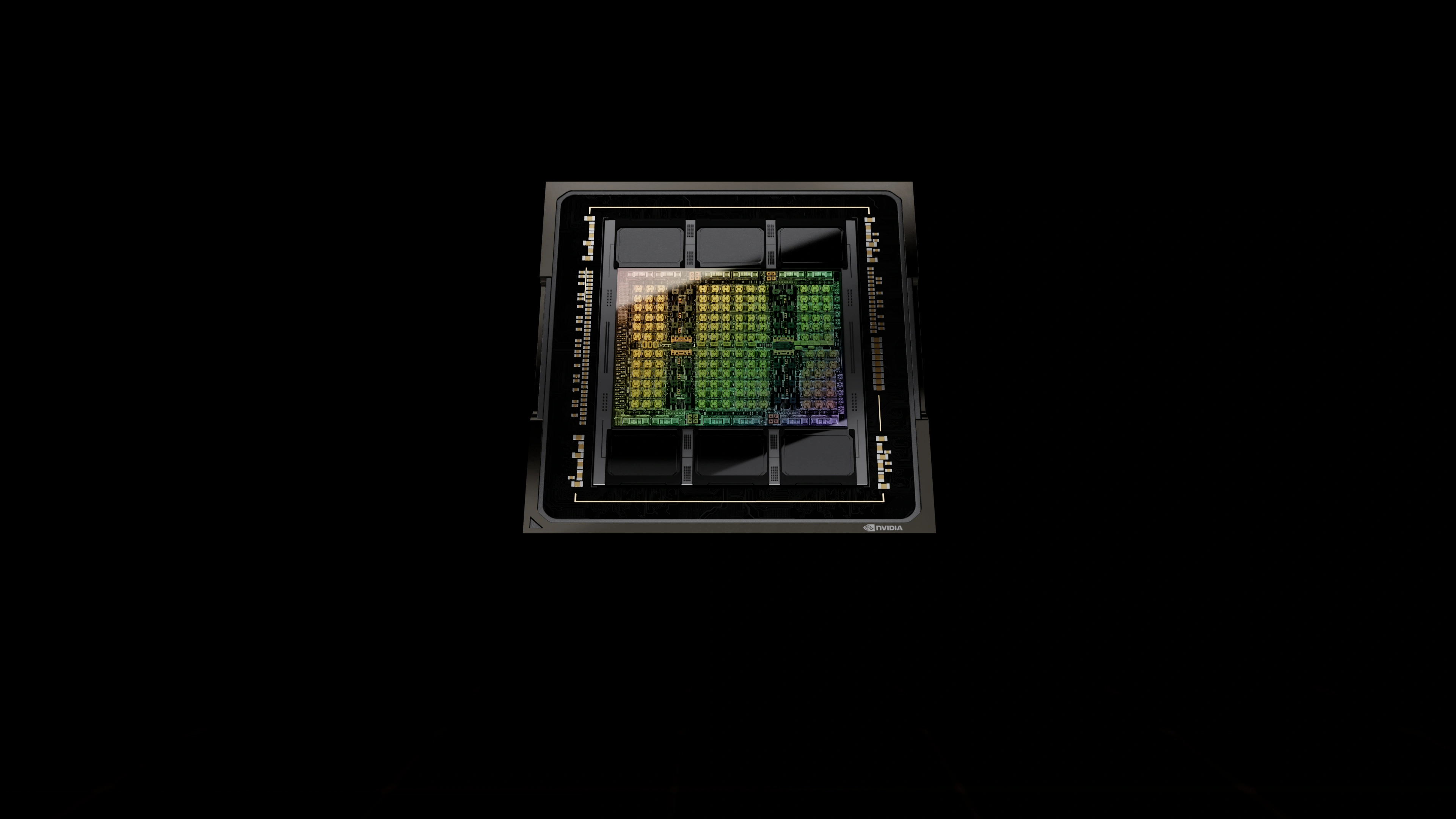 GH100 die present in all H100 GPUs
H100 PCIe
The H100 PCIe version is designed for simple deployment in standard servers. By fitting into existing PCIe Gen5 slots, it offers lower peak performance than its SXM counterpart and prioritizes flexibility.
- Lower power consumption.
- No NVLink bridge.
- Ideal for inference.
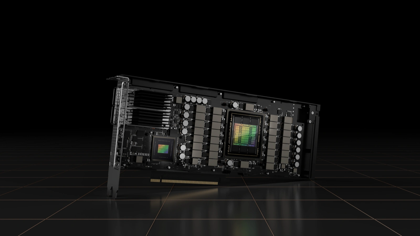 NVIDIA H100 PCIe without the chassis
H100 NVL
The H100 NVL pairs two H100 PCIe GPUs through NVLink, creating a tightly coupled configuration for large-scale inference workloads. It increases total available memory and enables high-bandwidth communication between GPUs. While memory is not fully unified, the fast interconnect improves multi-GPU performance for large models.
- Dual-GPU configuration
- High-bandwidth GPU-to-GPU interconnect
- Designed for LLM serving and recommendation systems
- Improved memory capacity for large models
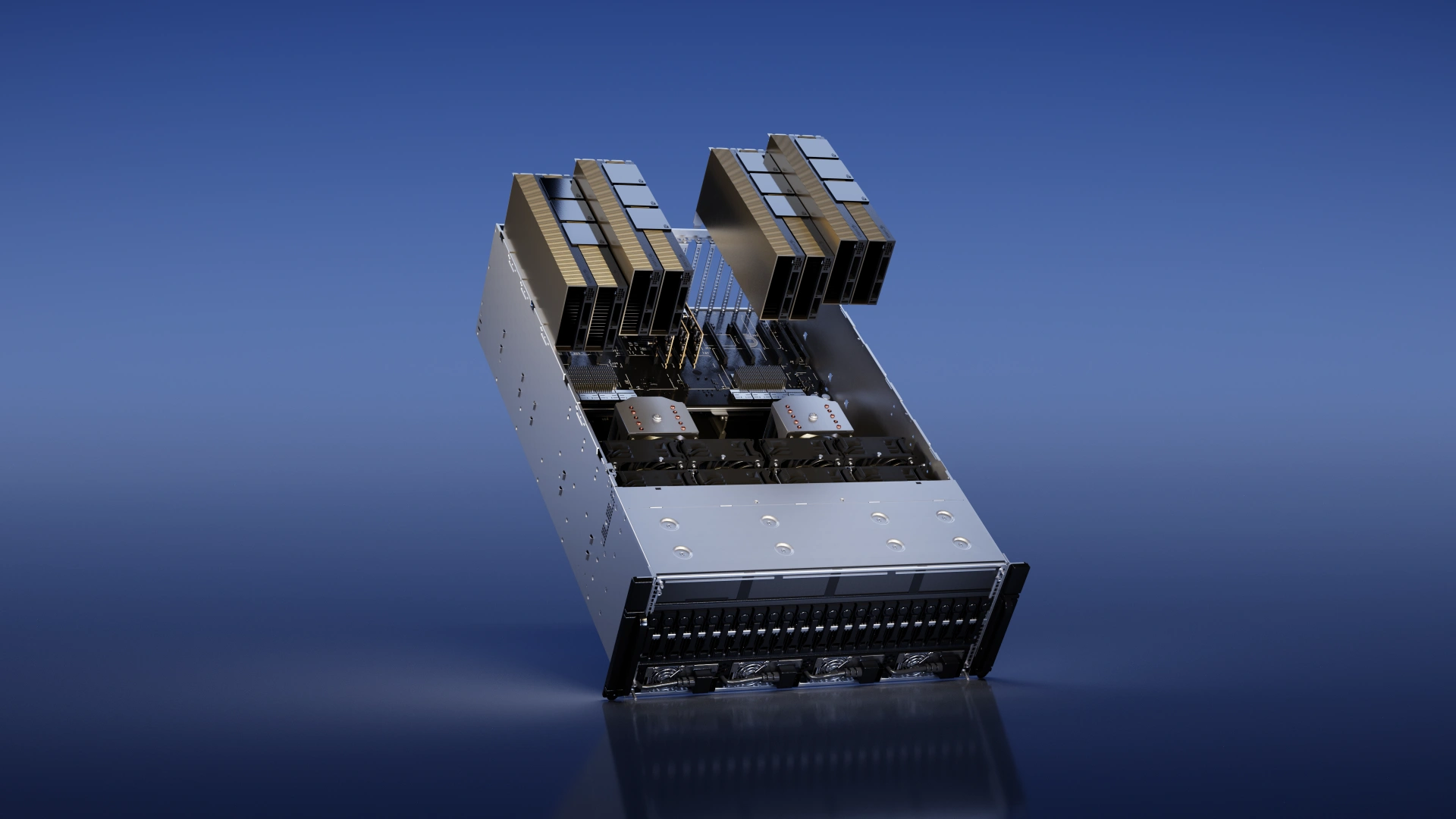 Server with NVIDIA NVL GPUs connected via NVLink
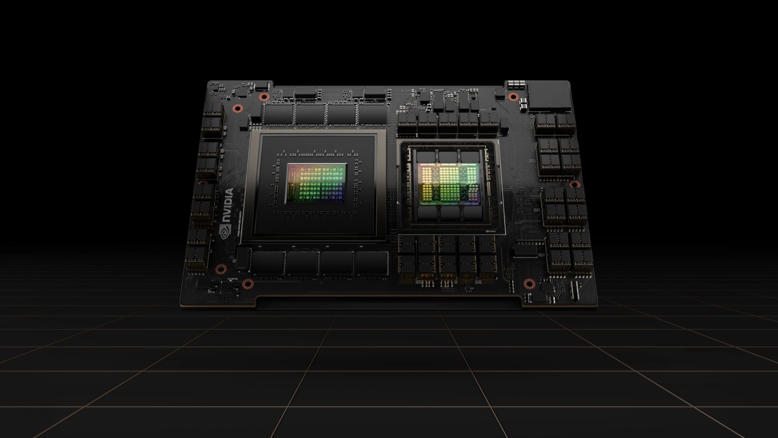
H100 SXM
The SXM form factor is built for maximum performance. It operates at significantly higher power levels and enables full NVLink connectivity, allowing GPUs to communicate at extremely high bandwidth with minimal latency. This makes it the preferred choice for large-scale AI training and workloads.
- Higher power consumption (700W).
- Full NVLink support.
- Used in HGX and DGX systems.
- Best for large-scale AI training.
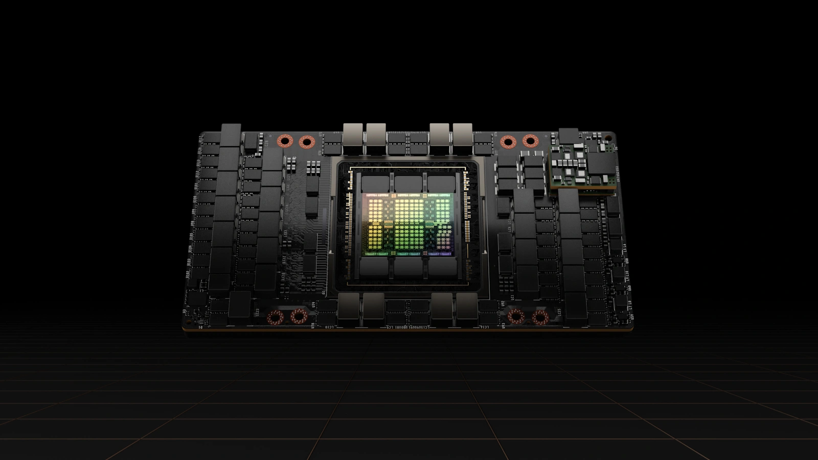 NVIDIA H100 SXM module
H100 Specifications
All H100 variants share the same underlying architecture and core feature set.
| Common Features For All H100 GPUs | |
|---|---|
| Architecture | Hopper |
| Die | GH100 |
| Tensor Core Generation | 4th |
| Compatibility | TensorRT, cuDNN, NCCL |
| AI Frameworks | PyTorch, TensorFlow, JAX |
Key specifications vary across form factors and configurations, particularly in memory, bandwidth, power, and interconnect. The table below compares the most important hardware and performance differences.
| Specification | H100 PCIe | H100 NVL | H100 SXM |
|---|---|---|---|
| CUDA Cores Count | 14,592 | 16,896 | 16,896 |
| VRAM | 80 GB HBM2e | 94 GB HBM3 | 80 GB HBM3 |
| Memory Bandwidth | 2.0 TB/s | ~3.9 TB/s | ~3.35 TB/s |
| FP64 (TFLOPS) | 26 | 30 | 34 |
| FP64 Tensor (TFLOPS) | 51 | 60 | 67 |
| FP32 (TFLOPS) | 51 | 60 | 67 |
| TF32 Tensor* (TFLOPS) | 756 | 835 | 989 |
| BF16 Tensor* (TFLOPS) | 1,513 | 1,671 | 1,979 |
| FP16 Tensor* (TFLOPS) | 1,513 | 1,671 | 1,979 |
| FP8 Tensor* (TFLOPS) | 3,026 | 3,341 | 3,958 |
| INT8 Tensor* (TOPS) | 3,026 | 3,341 | 3,958 |
| Power Consumption | ~350 W | ~350-400 W | Up to 700 W |
| Interconnect | PCIe Gen5 | NVLink + PCIe Gen5 | NVLink + PCIe Gen5 | * Shown with sparsity. Specifications 1/2 lower without sparsity. |
Sources
- These numbers highlight why the H100 remains a top-tier GPU for AI workloads in 2026.
- See NVIDIA's H100 product page for official platform details.
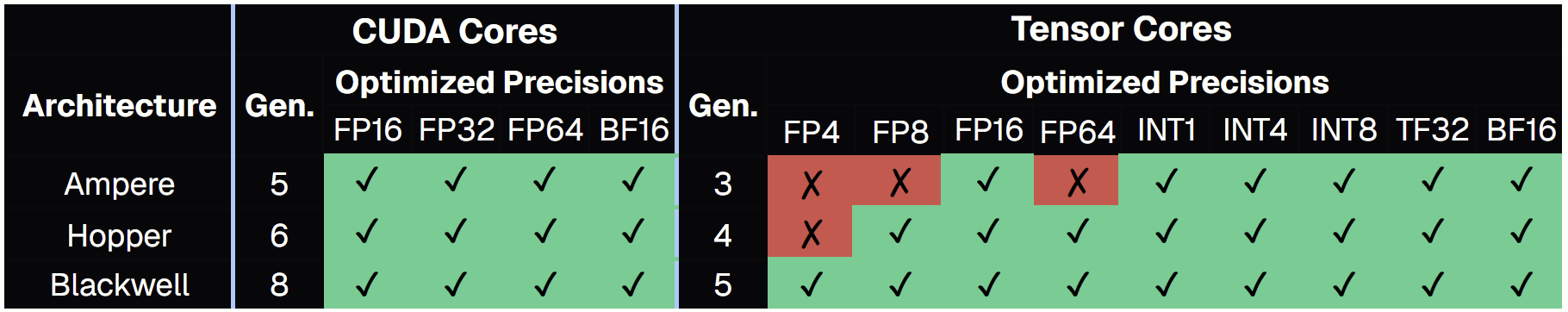
H100 Supported Precisions
The H100 introduces expanded support for lower-precision formats, improving throughput for AI tasks. Through its 4th generation Tensor Cores and Transformer Engine, it can select the optimal precision for an operation, balancing speed and accuracy.
- FP32: Traditional compute workloads
- FP16: Training deep learning models
- BF16: Improved numerical stability for training
- FP8: Breakthrough format for ultra-fast AI inference and training
FP8 is particularly important because it enables massive throughput gains while maintaining acceptable accuracy for many models.
Major differences between Hopper and other architectures:
- Compared to Ampere, Hopper is optimized for FP64 and FP8 Tensor Core calculations.
- The newer Blackwell architecture only adds FP4 support.
H100 Chips
GH100: GPU Chip
The GH100 is the core silicon behind all H100 GPUs, built specifically for large-scale AI and high-performance computing workloads. It combines massive parallelism and adds a Transformer Engine, enabling efficient execution of modern deep learning models across a range of precisions.
- Built on TSMC 4N process
- ~80 billion transistors
- Optimized for tensor operations and parallel compute
Given that the GH100 die powers all H100 variants, differences in performance between them come from power limits, memory, and interconnects.
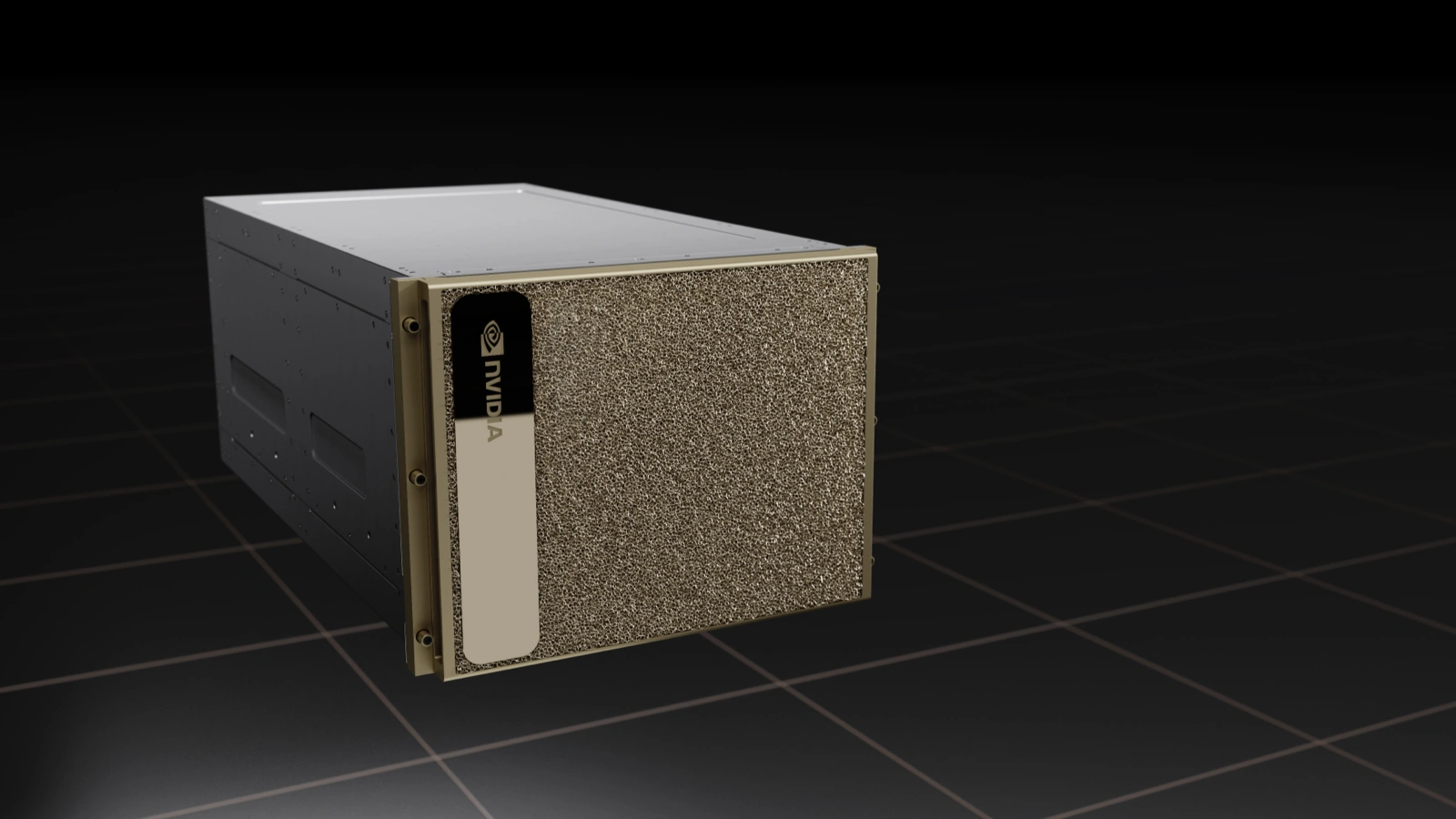
GH200: The Grace Hopper Superchip
The GH200 combines a GH100 GPU with a Grace CPU into a single superchip. Linking both components with NVLink-C2C enables high-bandwidth and low-latency communication.
- Unified memory architecture
- Designed for memory-intensive AI workloads
- Ideal for large-scale model training and inference
While NVIDIA had previously developed CPUs for mobile and embedded systems, Grace represents its first major push into data center CPUs, purpose-built for AI and high-performance computing workloads.
 NVIDIA Grace Hopper GH200 superchip
H100 Systems
H100 GPUs are typically part of integrated systems that combine multiple GPUs with high-speed interconnects, optimized power delivery, and cooling.
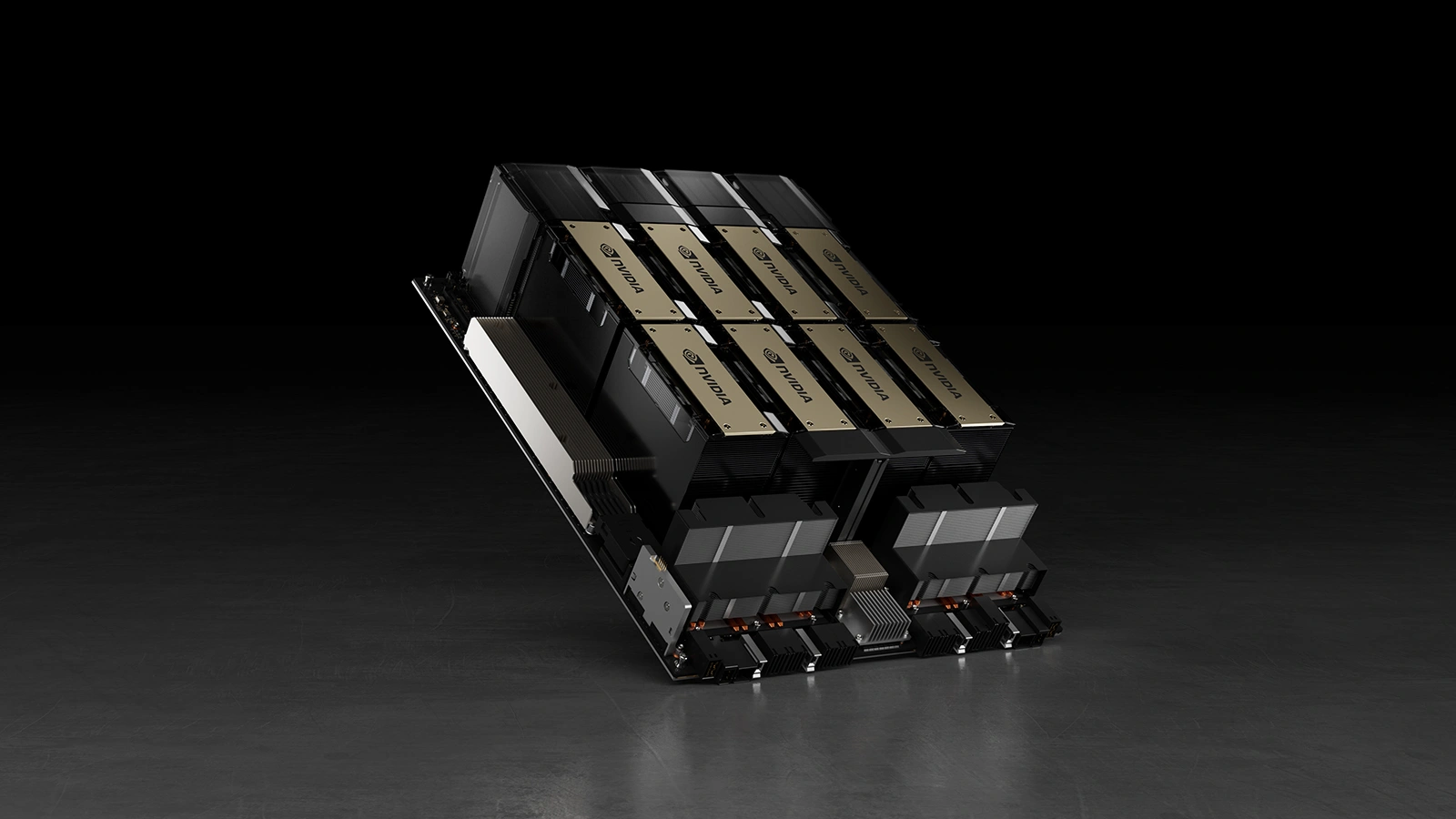
DGX H100
The DGX H100 integrates H100 SXM GPUs with optimized networking, storage, and software, making it a turnkey solution for scaling AI.
- 8x H100 SXM GPUs
- Dual x86 CPUs (Intel Xeon or AMD EPYC)
- Fully interconnected with NVLink
- Petaflop-scale AI performance
- Turnkey solution for enterprises
Common use cases include training large language models and foundation models.
 NVIDIA DGX H100 system
HGX H100
HGX is a modular platform used by cloud providers and OEMs. Unlike DGX systems, which are fully integrated, HGX provides the core GPU baseboard that partners build around with their hardware and infrastructure.
- Configurations with 4, 8, or more H100 GPUs
- NVLink-enabled GPU fabric
- Flexible deployment in hyperscale environments
HGX is designed for flexibility and scale, allowing providers to tailor infrastructure to specific workloads. As a result, HGX platforms form the backbone of most modern AI cloud environments.
 NVIDIA HGX platform
Why H100 Still Matters In 2026
Despite newer GPUs entering the market, the H100 remains a dominant AI workhorse due to:
- Strong performance across training and inference
- Wide availability in cloud environments
- Proven reliability in production workloads
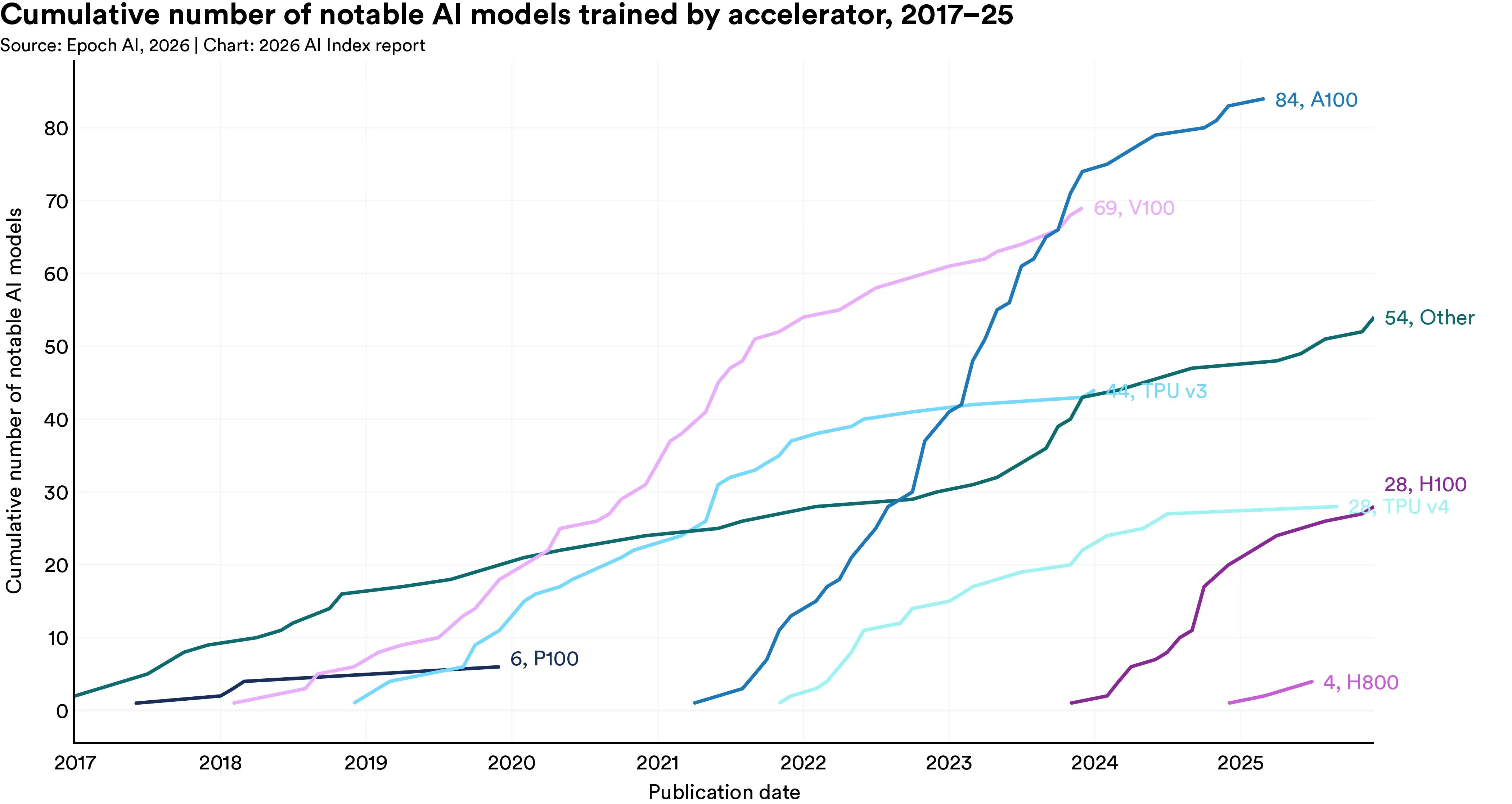
The H100's relevance is best illustrated by its adoption in high-stakes research. According to the 2026 AI Index Report, the H100 was used to train 28 notable AI models in 2025 alone. That number continues to climb as it replaces the A100 in new deployments.
* AI Index Report: 1.2 Compute and Infrastructure
Thunder Compute offers H100 PCIe GPUs starting at $1.38/hour, making high-performance AI compute accessible without long-term commitments.
Final Thoughts On H100 Specs
The NVIDIA H100 is still one of the most widely deployed AI GPUs for its strong tensor performance, high memory bandwidth, and a mature software ecosystem.
Across PCIe, SXM, and NVL configurations, it offers flexibility to match different workloads.
While newer architectures are beginning to push performance further, the H100 continues to strike a practical balance between performance, availability, and pricing.
To match the right hardware to your workload, see our GPU selection guide for AI workflows
FAQ
What are the main form factors of the NVIDIA H100?
The H100 comes in three primary form factors: PCIe (for standard servers), NVL (a dual-GPU PCIe setup optimized for LLMs), and SXM (designed for high-performance systems like DGX/HGX with full NVLink support).
What is the difference between H100 PCIe and H100 SXM?
The PCIe version is designed for flexible deployment in standard servers with lower power consumption (350W). In contrast, the SXM version is built for maximum performance, supporting higher power envelopes (up to 700W) and full NVLink connectivity for massive multi-GPU scaling.
Why is the H100 still widely used in 2026?
Even with newer GPUs like the B200 available, the H100 remains the industry workhorse due to its:
- Mature ecosystem: Strong software support and reliability.
- Availability: Widely accessible in cloud environments.
- Cost-Efficiency: Strikes the best balance between training performance and rental costs ($1.38/hour via Thunder Compute).