Released in 2022, the NVIDIA H100 debuted the Hopper architecture and delivered step-change gains in tensor performance, memory bandwidth, and efficiency over the A100.
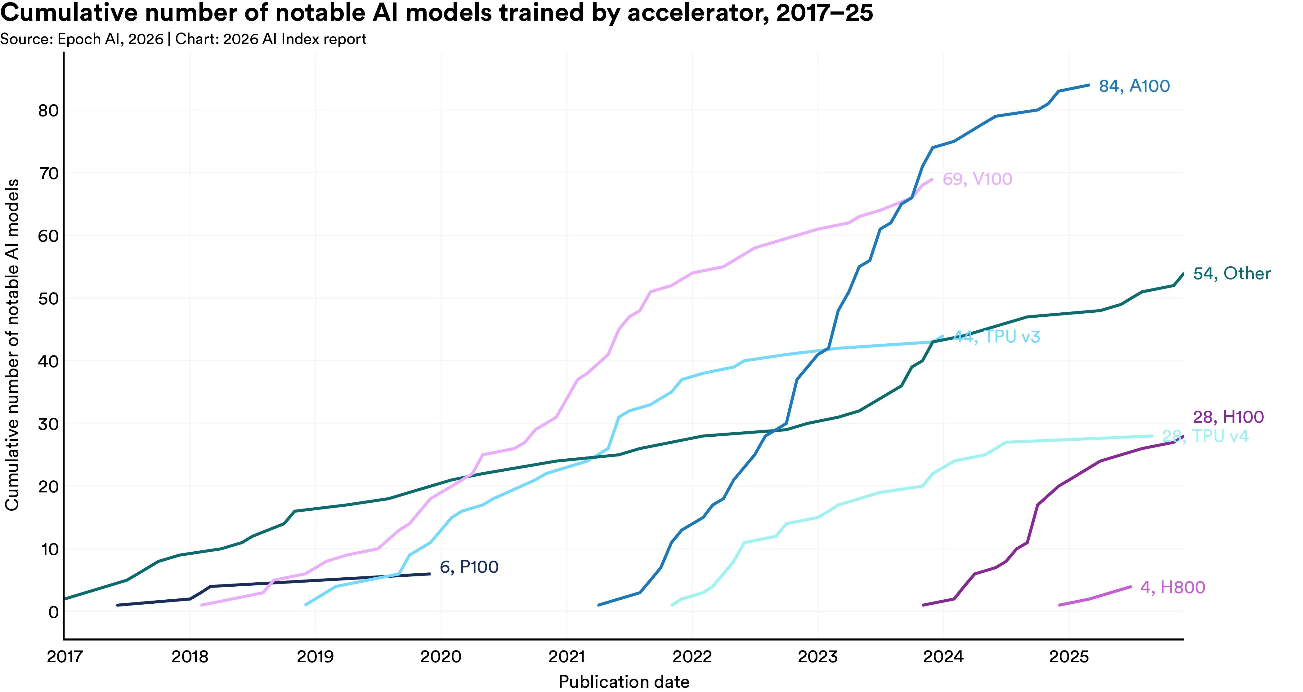
It remains the practical workhorse for most AI projects nearly four years later, having been used to train 28 notable AI models in 2025 alone, according to the 2026 AI Index Report.
Newer GPUs like the B200 have since entered the market, but they are expensive, scarce, and hard to rent. The H100 fills that gap. GH100 is the die name, but the products built around it vary significantly in memory, bandwidth, power, and interconnect.This guide covers all of it: form factors, full specifications, precision formats, MIG partitioning, real-world performance, and comparisons to the A100, H200, and Blackwell.
For pricing and provider comparisons, see the companion posts: NVIDIA H100 pricing and NVIDIA A100 vs H100.
H100 Form Factors
The H100 comes in two physical form factors (PCIe and SXM) plus a third specialized configuration (NVL):
- PCIe: For standard servers; no NVLink bridge, lower bandwidth, simpler deployment.
- NVL: A pre-configured dual-H100 PCIe setup with NVLink and more total memory per pair.
- SXM: Designed for high-performance systems; supports full NVLink connectivity and the highest bandwidth.
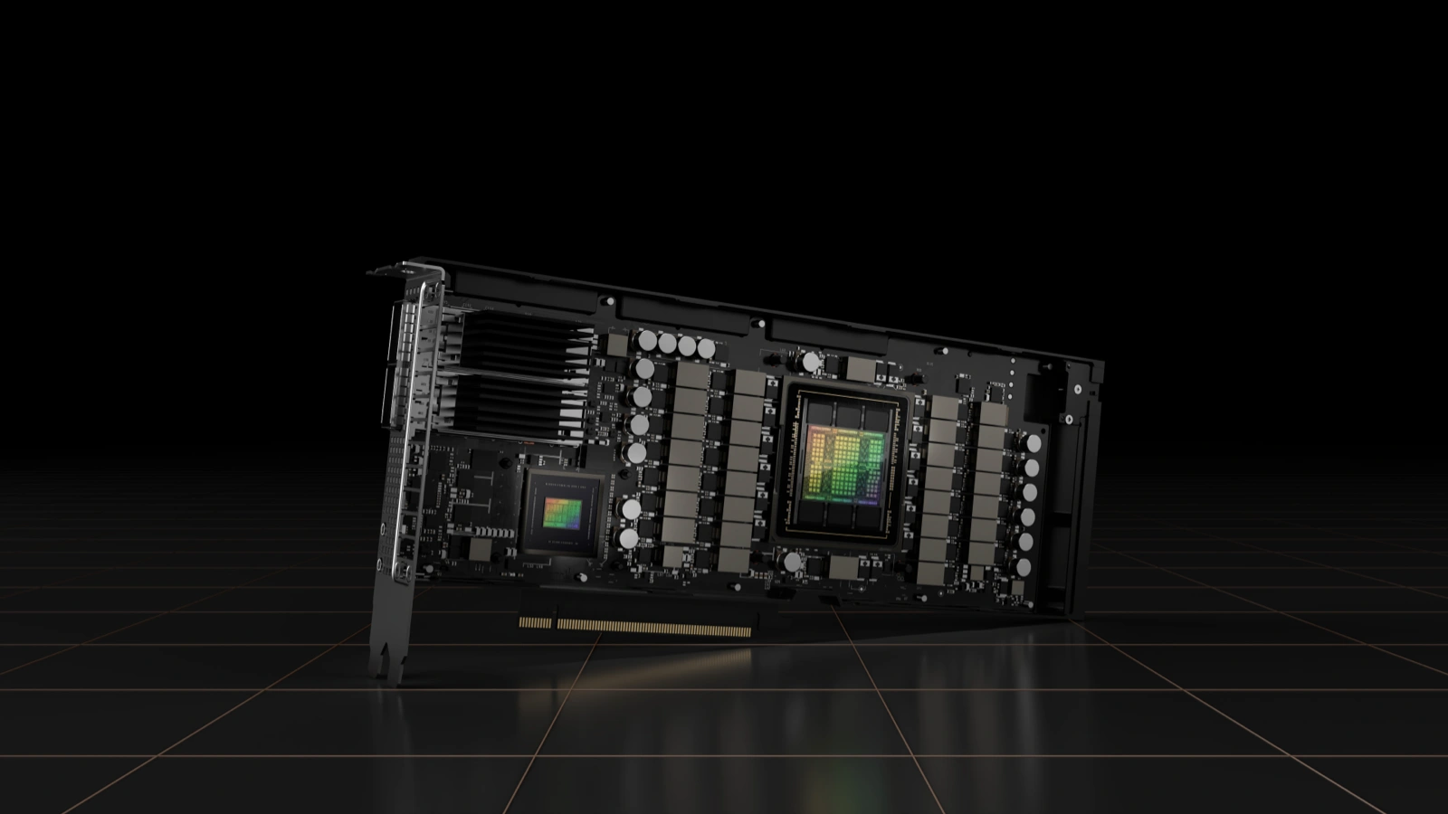
H100 PCIe
The H100 PCIe fits into existing PCIe Gen5 server slots and prioritizes flexible deployment over peak performance. It draws around 350W and operates without a NVLink bridge, making it the most practical option for single-GPU inference or fine-tuning.
The H100 PCIe Product Brief confirms a 350W TDP and memory bandwidth exceeding 2,000 GB/s.
- Lower power consumption (350W TDP)
- No NVLink bridge
- Ideal for inference and single-GPU workloads
H100 NVL
The H100 NVL pairs two H100 PCIe GPUs through NVLink into a tightly coupled configuration for large-scale inference. It provides 94 GB HBM3 per GPU at 3.9 TB/s bandwidth, making it well suited for LLM serving and recommendation systems that push beyond what a single PCIe card can handle.
The H100 NVL Product Brief lists a 400W TDP and memory bandwidth of nearly 4,000 GB/s.
- Dual-GPU configuration
- 94 GB HBM3 per GPU at 3.9 TB/s bandwidth
- High-bandwidth GPU-to-GPU interconnect
- Designed for LLM serving and recommendation systems
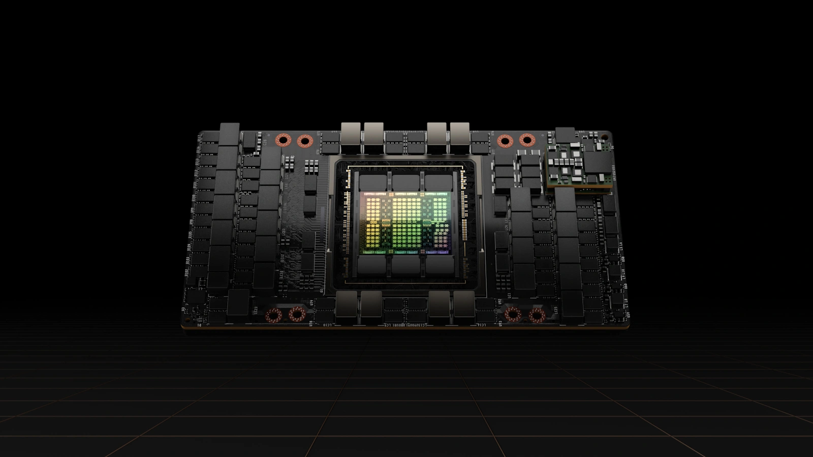
H100 SXM
The SXM form factor is built for maximum performance. It operates at up to 700W and enables full NVLink 4.0 connectivity, allowing GPUs to communicate at 900 GB/s with minimal latency. This is the variant used in DGX and HGX systems for large-scale AI training.
- Up to 700W TDP
- Full NVLink 4.0 support (900 GB/s per GPU)
- Used in HGX and DGX systems
- Best for distributed, multi-GPU training
H100 Specifications
All H100 variants share the same underlying Hopper architecture and GH100 die. Specifications diverge across form factors in memory type, bandwidth, CUDA core count, and interconnect.
| Common Features For All H100 GPUs | |
|---|---|
| Architecture | Hopper |
| Die | GH100 |
| Tensor Core Generation | 4th |
| Compatibility | TensorRT, cuDNN, NCCL |
| AI Frameworks | PyTorch, TensorFlow, JAX |
NVIDIA's official datasheet leads with sparsity-enabled figures. Dense (non-sparsity) values are half the listed TFLOPS and reflect what you get without explicit 2:4 structured sparsification of the model weights. Most production workloads use dense values.
| Specification | H100 PCIe | H100 NVL | H100 SXM |
|---|---|---|---|
| Streaming Multiprocessors | 114 SMs | 132 SMs per GPU | 132 SMs |
| CUDA Cores | 14,592 | 16,896 | 16,896 |
| Tensor Cores (4th Gen) | 456 | 528 | 528 |
| VRAM | 80 GB HBM2e | 94 GB HBM3 | 80 GB HBM3 |
| Memory Bandwidth | 2.0 TB/s | ~3.9 TB/s | ~3.35 TB/s |
| L2 Cache | 50 MB | 50 MB | 50 MB |
| FP64 (TFLOPS) | 26 | 30 | 34 |
| FP64 Tensor (TFLOPS) | 51 | 60 | 67 |
| FP32 (TFLOPS) | 51 | 60 | 67 |
| TF32 Tensor* (TFLOPS) | 756 | 835 | 989 |
| BF16 Tensor* (TFLOPS) | 1,513 | 1,671 | 1,979 |
| FP16 Tensor* (TFLOPS) | 1,513 | 1,671 | 1,979 |
| FP8 Tensor* (TFLOPS) | 3,026 | 3,341 | 3,958 |
| INT8 Tensor* (TOPS) | 3,026 | 3,341 | 3,958 |
| Power Consumption | ~350W | ~350–400W | Up to 700W |
| NVLink | PCIe Gen5 only | NVLink + PCIe Gen5 | NVLink 4.0 + PCIe Gen5 |
| NVLink Bandwidth | N/A | ~600 GB/s | 900 GB/s per GPU |
| MIG Support | Up to 7 instances | Up to 7 instances | Up to 7 instances |
| * Shown with sparsity. Dense values are half the listed figure. | |||
Sources: NVIDIA H100 Datasheet | NVIDIA H100 Product Page
Thunder Compute offers H100 PCIe GPUs starting at $1.38/hr, with no long-term commitments and no infrastructure setup required.
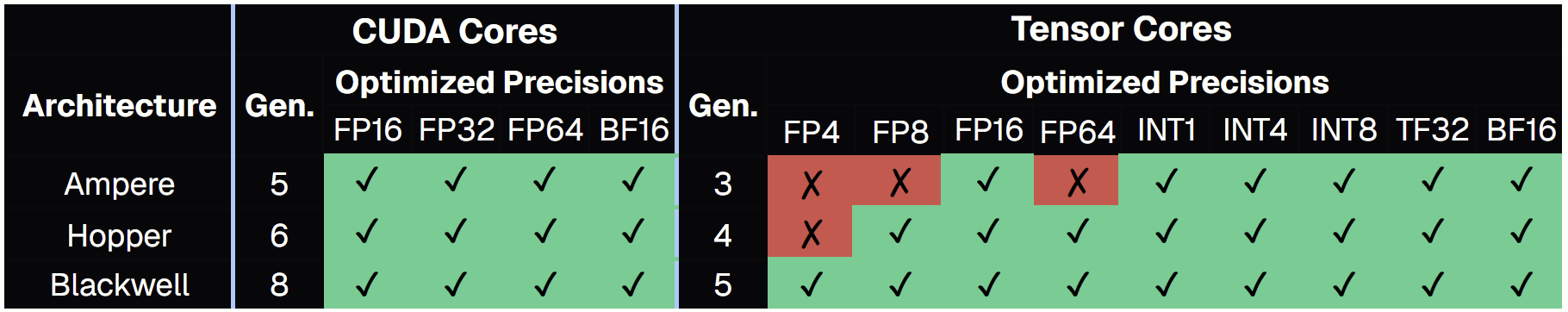
H100 Supported Precisions and the Transformer Engine
The H100 expands precision support through its 4th-generation Tensor Cores and a dedicated Transformer Engine.
The Transformer Engine is the most important architectural addition in Hopper. It automatically selects between FP8 and FP16 precision on a per-operation basis during training, with no manual intervention required. On transformer-based models like GPT and LLaMA, this delivers 3-4x the throughput of the A100, as described in the NVIDIA H100 product page.
Frameworks including vLLM, TensorRT-LLM, and the transformer_engine PyTorch package unlock this gain automatically; stacks that fall back to BF16 do not.
The full precision stack the H100 supports:
- FP64: Scientific and HPC workloads
- FP32: Traditional deep learning compute
- TF32: Drop-in replacement for FP32 with higher throughput on Tensor Cores
- FP16: Standard deep learning training
- BF16: Numerically stable alternative to FP16 for training
- FP8: Highest-throughput format for LLM training and inference (Hopper-exclusive)
- INT8: Quantized inference
FP8 delivers throughput roughly double that of FP16 while maintaining acceptable accuracy for most LLM workloads. FP8 tooling on H100 is production-proven across PyTorch, vLLM, and TensorRT-LLM, which is a maturity advantage over newer Blackwell hardware.
H100 vs A100: Key Differences
The H100 is a substantial generational leap over the A100, not a minor refresh. The table below covers the most important differences for teams evaluating both.
| Specification | H100 SXM | A100 SXM | Notes |
|---|---|---|---|
| Architecture | Hopper (GH100) | Ampere (GA100) | Different die and process |
| VRAM | 80 GB HBM3 | 80 GB HBM2e | Same capacity, faster type on H100 |
| Memory Bandwidth | 3.35 TB/s | 2.0 TB/s | 68% faster on H100 |
| FP16 TFLOPS (dense) | 989 | 624 | ~1.6x higher on H100 |
| FP8 TFLOPS (dense) | 1,979 | N/A | FP8 is H100-exclusive |
| Transformer Engine | Yes (FP8/FP16 auto-switching) | No | Defines H100's LLM advantage |
| NVLink Generation | NVLink 4.0 (900 GB/s) | NVLink 3.0 (600 GB/s) | 50% more inter-GPU bandwidth on H100 |
| MIG Support | Up to 7 instances | Up to 7 instances | Equivalent partition count |
| Confidential Computing | Yes (hardware TEE) | No | H100 is first GPU with on-die TEE |
| Purchase price (2026)1 | $25,000–$40,000 | $10,000–$15,000 | Secondary market estimates |
| 1 Secondary market pricing as of Q2 2026. Subject to change. | |||
For a full breakdown, see the NVIDIA A100 vs H100 comparison guide.
H100 vs H200: What Changed
The H200 uses the same GH100 compute die as the H100. CUDA core count, Tensor Core count, and FP8/FP16 compute performance are identical. The upgrade is entirely in the memory subsystem.
| Specification | H100 SXM | H200 SXM |
|---|---|---|
| Die | GH100 | GH100 |
| VRAM | 80 GB HBM3 | 141 GB HBM3e |
| Memory Bandwidth | 3.35 TB/s | ~4.8 TB/s |
| FP8 TFLOPS (with sparsity) | 3,958 | 3,958 |
| CUDA Cores | 16,896 | 16,896 |
| Transformer Engine | Yes | Yes |
| Power (TDP) | 700W | 700W |
For workloads that fit within 80 GB VRAM, H100 and H200 perform nearly identically. The H200's 141 GB matters for models that exceed 80 GB at full precision, very long context windows, or large-batch inference where capacity is the binding constraint.
MIG: Running Multiple Workloads on One H100
Multi-Instance GPU (MIG) partitions a single H100 into up to 7 fully isolated GPU instances. Each instance receives a dedicated slice of CUDA cores, Tensor Cores, L2 cache, and HBM memory with hardware-enforced isolation. MIG instances appear as separate GPU devices to the OS, so each runs its own container independently.
On the H100 SXM5, a full 7-way partition gives each instance approximately 10 GB HBM3 and 2,048 CUDA cores. The two most common production patterns are:
- 7x 1g.10gb: Multi-tenant inference of small models (Mistral 7B, Llama 3 8B) with per-job cost efficiency
- 2x 3g.40gb: Two simultaneous 13B model servers with balanced memory and compute
MIG is most valuable for inference teams where a full 80 GB GPU is more than any single request needs. At Thunder Compute, H100 PCIe instances are available from $1.38/hr with no minimum commitment, making MIG-style workload splitting accessible for most inference use cases.
H100 Confidential Computing
The H100 was the first GPU to implement hardware-enforced confidential computing, using an on-die Trusted Execution Environment (TEE). Data transfers between CPU and GPU are encrypted using AES-256, executed on-die. A peer-reviewed benchmark study (arXiv 2409.03992) found the average overhead is below 7%, and efficiency approaches 99% for large models like Llama 3.1-70B, where GPU compute time dominates over I/O overhead.
This is particularly relevant for regulated industries: healthcare (HIPAA-sensitive model training), finance (proprietary model IP), and government (sensitive inference workloads). For most developer use cases, confidential computing is not required, but it is the only feature of its kind available in any GPU generation prior to Hopper.
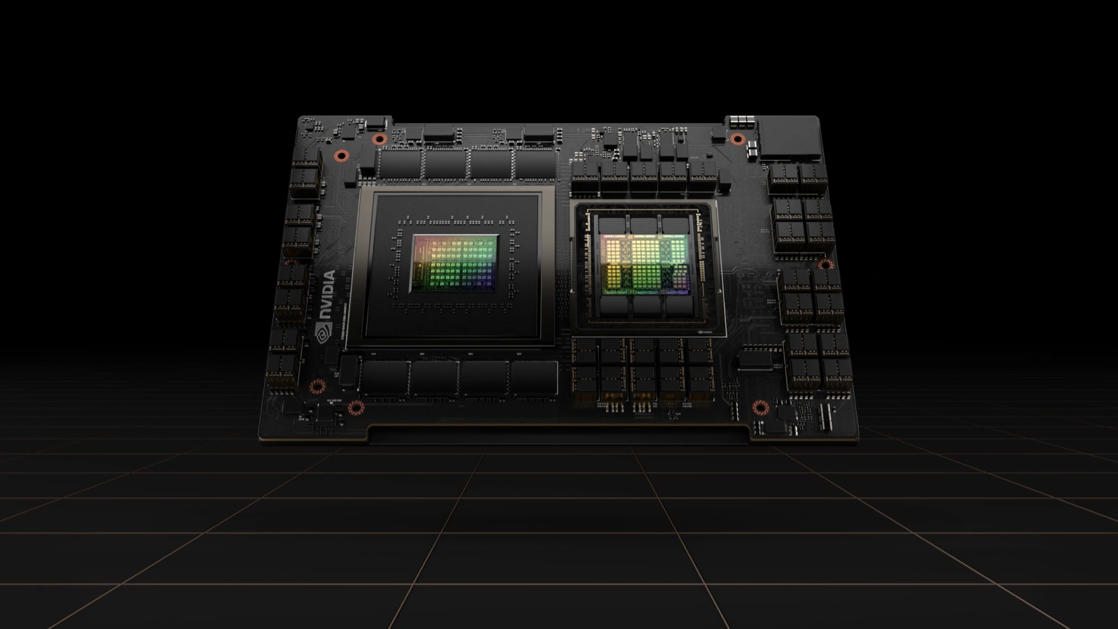
H100 Chips
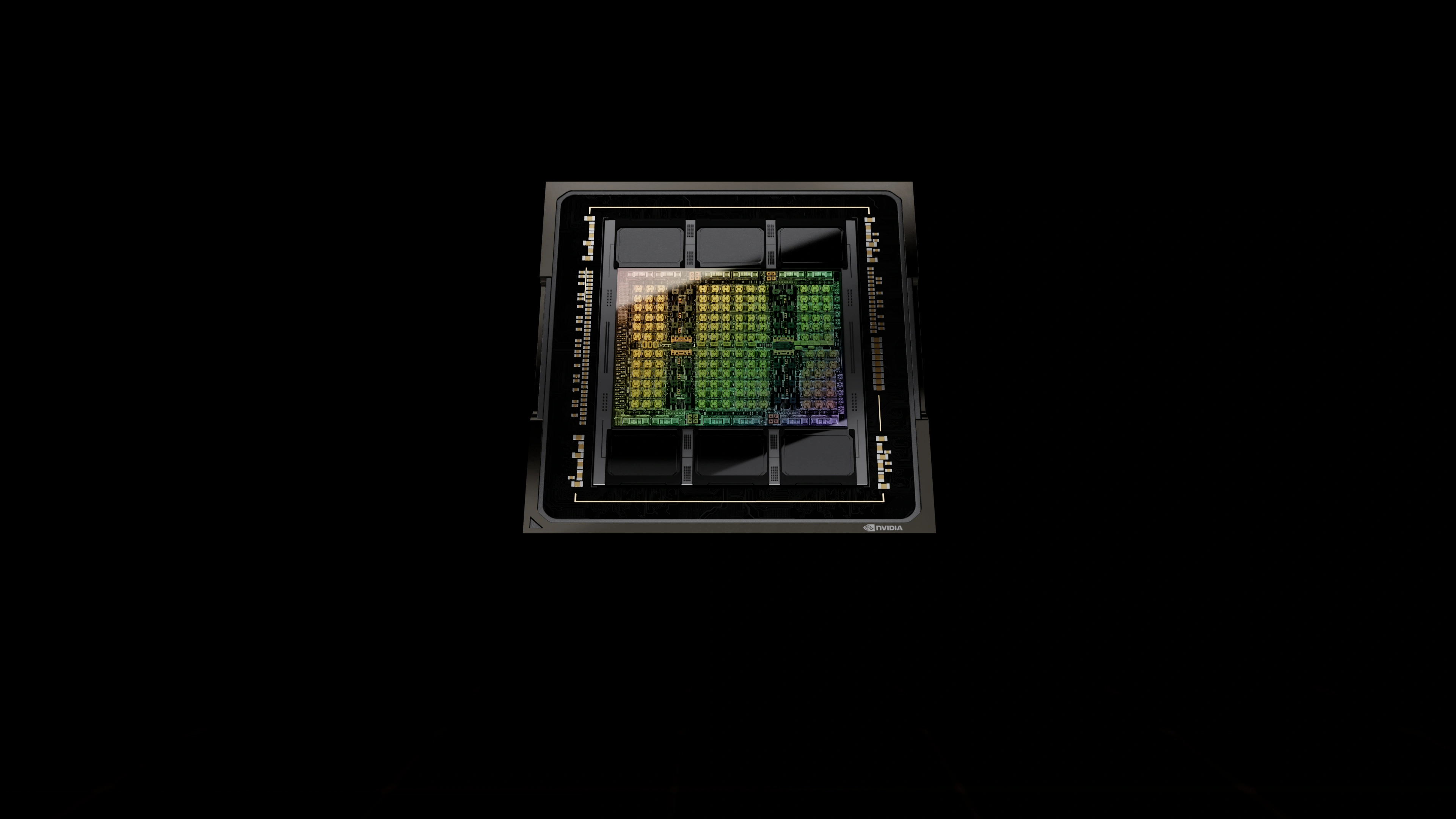
GH100: GPU Chip
The GH100 is the core silicon behind all H100 GPUs, built specifically for large-scale AI and high-performance computing workloads. It combines massive parallelism and adds a Transformer Engine, enabling efficient execution of modern deep learning models across a range of precisions.
- Built on TSMC 4N process
- ~80 billion transistors
- Optimized for tensor operations and parallel compute
Given that the GH100 die powers all H100 variants, differences in performance between them come from power limits, memory, and interconnects.
GH200: The Grace Hopper Superchip
The GH200 combines a GH100 GPU with NVIDIA's Grace ARM CPU into a single superchip, connected via NVLink-C2C at 900 GB/s. This design enables a unified memory architecture that dramatically increases the effective bandwidth available to applications running across both CPU and GPU.
- Unified memory architecture
- Designed for memory-intensive AI and HPC workloads
- Ideal for models requiring terabyte-scale memory access
While NVIDIA had previously developed CPUs for mobile and embedded systems, Grace represents its first major push into data center CPUs, purpose-built for AI and high-performance computing workloads.
H100 Real-World Performance
The H100's advantage over the A100 comes from three compounding improvements: the Transformer Engine's FP8 precision, 68% higher memory bandwidth on the SXM variant, and NVLink 4.0's 50% increase in inter-GPU bandwidth. In practice, H100 clusters have reduced large-model training times by 2 to 3 times compared to equivalent A100 configurations. For inference, gains of 2 to 4 times on large transformer models are common, depending on model size and batch configuration.
According to NVIDIA's SemiAnalysis InferenceX benchmarks from April 2026, H100 delivers inference at approximately $0.09 per 1M tokens for a 120B parameter model using vLLM. At Thunder's $1.38/hr rate, this makes H100 one of the most cost-efficient inference options currently available.
The H100 was used to train 28 notable AI models in 2025 alone, a figure that continues to rise as it replaces A100 in new deployments, per the 2026 AI Index Report.
H100 Systems
H100 GPUs are typically deployed as part of integrated systems that combine multiple GPUs with high-speed interconnects, optimized power delivery, and coordinated cooling.
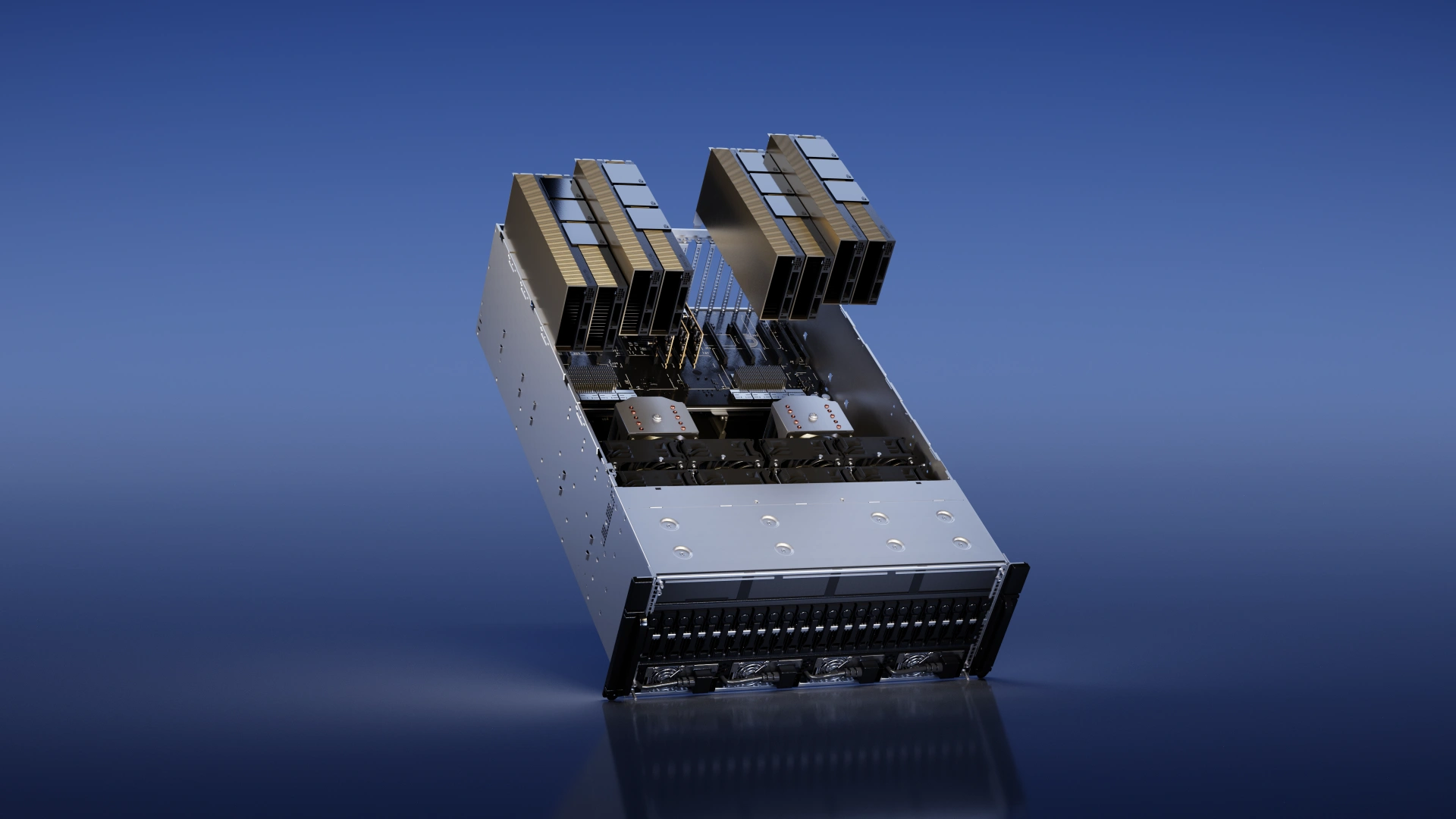
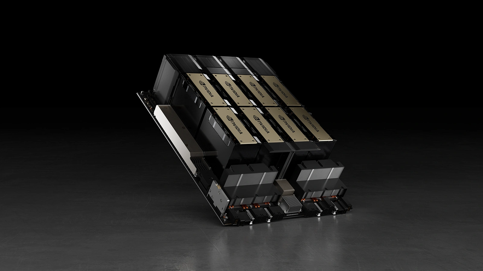
DGX H100
The DGX H100 integrates 8 H100 SXM GPUs with dual x86 CPUs (Intel Xeon or AMD EPYC), optimized networking, and storage in a fully interconnected, turnkey configuration.
It's designed as a single-node foundation for large language model training. A complete DGX H100 system costs approximately $300,000 to $400,000 new, based on 2026 market pricing data.
- 8x H100 SXM GPUs
- Dual x86 CPUs (Intel Xeon or AMD EPYC)
- Fully interconnected with NVLink
- Petaflop-scale AI performance
HGX H100
HGX is a modular platform used by cloud providers and OEMs. Unlike DGX systems, which are fully integrated, HGX provides the core GPU baseboard that partners build around with their hardware and infrastructure.
- Configurations with 4, 8, or more H100 GPUs
- NVLink-enabled GPU fabric. HGX platforms form the backbone of most modern AI cloud infrastructure, and most H100 instances available from cloud GPU providers are built on HGX-class hardware.
H100 Pricing and Cloud Access in 2026
Purchasing H100 hardware outright is expensive. H100 PCIe cards sell for approximately $25,000 to $30,000 through authorized resellers; full DGX H100 systems run $300,000 to $400,000. Secondary market SXM units trade between $6,000 and $15,000 as Blackwell supply expands, but lead times vary significantly.
For most developers and teams, renting on-demand is the practical path. Cloud rental rates have dropped from a 2023 peak of $8 to $12/hr to a 2026 market median around $2.29/hr, with hyperscalers still pricing in the $6 to $11 range.
| Provider Tier | H100 Rental Rate (2026)1 | Notes |
|---|---|---|
| Thunder Compute | From $1.38/hr (PCIe) | No minimum commitment, VS Code + Cursor extensions, one-click templates |
| Market median (independent providers) | ~$2.29/hr | Fluence, Spheron, Vast.ai, RunPod range |
| Hyperscalers (AWS, GCP, Azure) | $6–$11/hr | Higher availability guarantees, higher overhead cost |
| 1 Last update: June 24, 2026. Spot instances available at lower rates with interruption risk. | ||
Beyond pricing, the development workflow matters. Thunder Compute provides VS Code and Cursor extensions that connect you to an H100 instance directly from your IDE, plus one-click templates for image generation and local LLM serving. It is the fastest path to a running H100 environment without any infrastructure setup.
See Thunder Compute's current H100 availability and pricing →
Why the H100 Still Matters in 2026
The Blackwell B200 offers higher raw throughput, but it requires liquid cooling, draws significantly more power, and commands a substantial price premium.
Most existing training pipelines were built on H100, and migrating to Blackwell carries real engineering cost. H100 rental rates have also fallen 64 to 75% from their 2023 peak, making the hardware more cost-accessible than at any point since launch.
For teams whose models fit in 80 GB and whose workloads run efficiently on the existing CUDA/FP8 stack, the H100 is the clear practical choice in 2026. For frontier-scale training runs that require maximum throughput per GPU-hour, B200 may justify the premium, but availability remains constrained.
Last Thoughts on NVIDIA H100 Specs
The H100 remains the de facto standard for large-model training and production inference. Its Transformer Engine, 80 GB of high-bandwidth memory, and NVLink 4.0 interconnect cover everything from single-GPU fine-tuning to distributed training at scale.
At $1.38/hr on Thunder Compute, with VS Code and Cursor IDE integration and one-click templates, getting from zero to a running H100 environment takes minutes.
Get started with an H100 on Thunder Compute →
To match the right GPU to your workload, see the GPU selection guide for AI workflows.
FAQ
What are the main form factors of the NVIDIA H100?
The H100 comes in three configurations: PCIe (standard servers, no NVLink, 350W), NVL (dual PCIe GPUs bridged via NVLink, 94 GB HBM3 per GPU), and SXM (high-performance module with full NVLink 4.0, 700W TDP, used in DGX and HGX systems).
What is the difference between H100 PCIe and H100 SXM?
The PCIe variant uses HBM2e at ~2 TB/s bandwidth, draws 350W, and fits in standard servers without NVLink support. The SXM variant uses HBM3 at 3.35 TB/s, draws up to 700W, and supports NVLink 4.0 at 900 GB/s for multi-GPU training. PCIe is the right choice for inference and single-GPU workloads; SXM is the right choice for distributed training at scale.
How does the H100 Transformer Engine work?
The Transformer Engine automatically selects between FP8 and FP16 precision on a per-operation basis during training, without manual tuning. For transformer-based models, this delivers 3 to 4 times the throughput of the A100 at FP16. Framework support as of 2026 includes vLLM (--dtype fp8), TensorRT-LLM (native FP8 engine), and the transformer_engine package for PyTorch training.
What is MIG on the H100 and what workloads benefit?
MIG (Multi-Instance GPU) partitions one H100 into up to 7 isolated instances, each with a dedicated slice of CUDA cores, Tensor Cores, L2 cache, and HBM memory. Common patterns are 7x 1g.10gb for multi-tenant inference of small models and 2x 3g.40gb for two simultaneous 13B model servers. MIG is most useful for inference teams where a full 80 GB GPU is more than any single request needs.
How does the H100 compare to the H200?
The H200 uses the identical GH100 compute die, so CUDA cores, Tensor Cores, and FP8 throughput are the same. The upgrade is memory: 141 GB HBM3e at ~4.8 TB/s versus 80 GB HBM3 at 3.35 TB/s on the SXM H100. For workloads that fit in 80 GB, performance is nearly identical. The H200 adds value only for models exceeding 80 GB at full precision, very long context windows, or memory-bound large-batch inference.
How does the H100 compare to the A100?
The H100 delivers 3 to 4 times the throughput on transformer workloads via FP8 and the Transformer Engine, 68% more memory bandwidth on the SXM variant (3.35 vs 2.0 TB/s), and 50% more NVLink bandwidth (900 vs 600 GB/s). The A100 remains cost-competitive for workloads that don't require FP8 where the H100 price premium is not justified. See the full A100 vs H100 comparison for a detailed breakdown.
What is the H100's inference cost per token?
According to NVIDIA's SemiAnalysis InferenceX benchmarks from April 2026, the H100 delivers inference at approximately $0.09 per 1M tokens for a 120B parameter model using vLLM. At Thunder Compute's $1.38/hr rate, this makes H100 one of the most cost-efficient inference options available from a cloud provider.
What is the H100's confidential computing capability?
The H100 was the first GPU with hardware-enforced confidential computing via an on-die Trusted Execution Environment (TEE). Data transfers between CPU and GPU are AES-256 encrypted on-die. A peer-reviewed benchmark study found the average overhead is below 7%, approaching zero for large models like Llama 3.1-70B. This makes it suitable for HIPAA, finance, and government workloads.