Released in 2020, the NVIDIA A100 is a data center GPU built on NVIDIA's Ampere architecture. It became the standard GPU for AI model training from 2020 through 2023 and remains widely deployed on cloud infrastructure today.
This guide covers the full NVIDIA A100 GPU specifications across all four variants, chip architecture, supported precisions, use cases, and how it compares to the H100 in 2026.
NVIDIA A100 Form Factors
The A100 is available in two distinct form factors: PCIe and SXM. The choice between them directly affects thermal design, bandwidth, and peak performance.
NVIDIA A100 PCIe
The PCIe variant fits into standard server motherboards using a PCIe 4.0 x16 interface. It comes in 40 GB HBM2 and 80 GB HBM2e configurations and draws up to 300W through the PCIe slot and auxiliary power connectors.
Passive cooling and reliance on server chassis airflow make it easy to integrate into existing infrastructure.
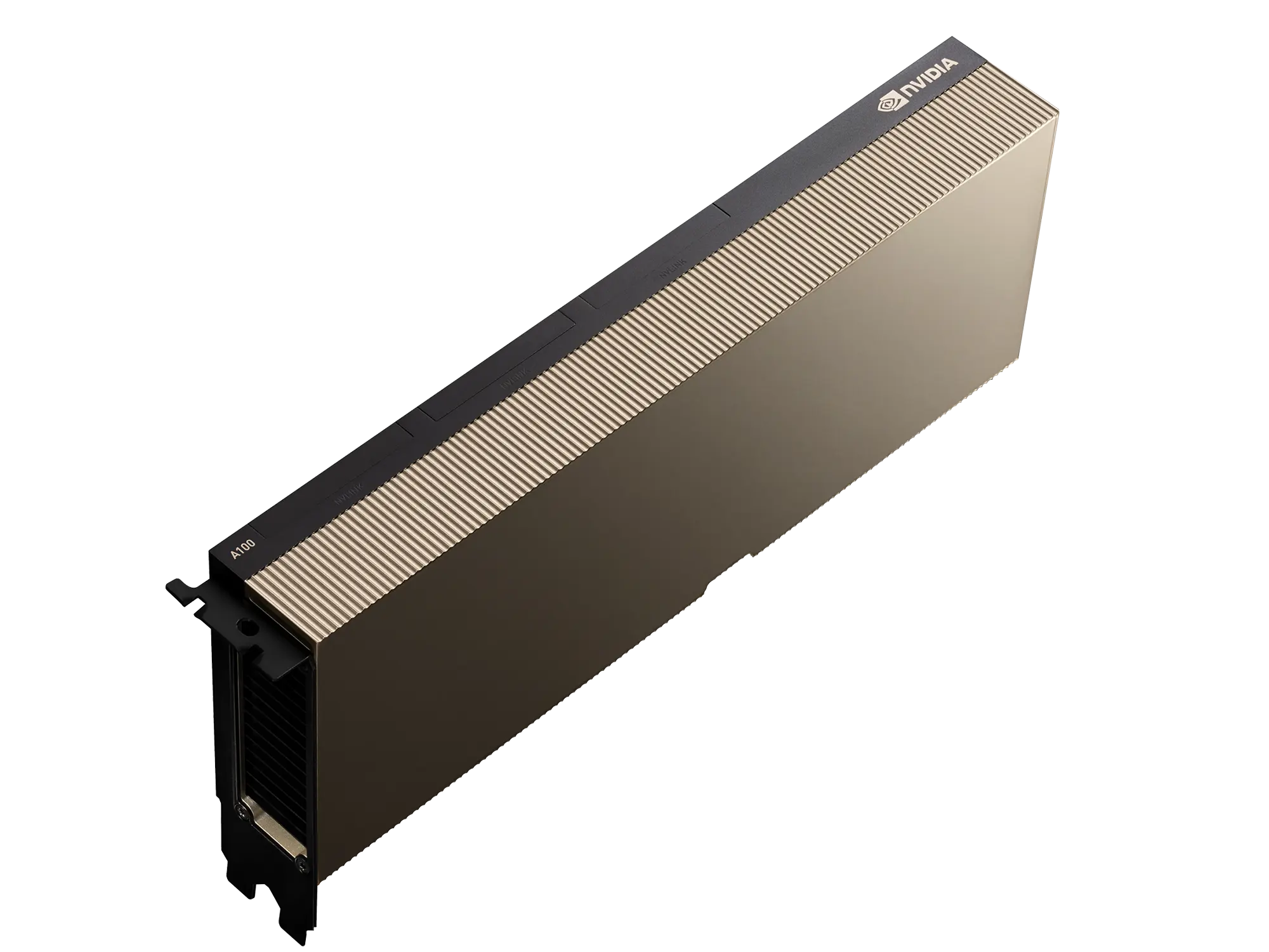
NVIDIA A100 SXM
The SXM4 variant mounts directly to NVIDIA's NVLink Switch System baseboard, enabling tighter GPU-to-GPU interconnects and a higher power envelope of 400W.
This thermal headroom translates into improved clock speeds and memory bandwidth compared to the PCIe version. The SXM form factor is the basis for NVIDIA's DGX and HGX systems and the preferred choice for maximum multi-GPU throughput.
NVIDIA A100 Specifications
The table below shows key NVIDIA A100 specs across form factors and memory configurations.
| Specification | A100 PCIe 40GB | A100 PCIe 80GB | A100 SXM 40GB | A100 SXM 80GB |
|---|---|---|---|---|
| Architecture | Ampere (GA100) | |||
| Process Node | TSMC 7nm | |||
| CUDA Cores | 6,912 | |||
| Tensor Cores (3rd Gen) | 432 | |||
| GPU Boost Clock | 1,410 MHz | |||
| FP64 (CUDA Core) | 9.7 TFLOPS | 9.7 TFLOPS | 19.5 TFLOPS | 19.5 TFLOPS |
| FP64 (Tensor Core) | 19.5 TFLOPS | 19.5 TFLOPS | ||
| FP32 | 19.5 TFLOPS | |||
| A100 VRAM | 40GB HBM2 | 80GB HBM2e | 40GB HBM2 | 80GB HBM2e |
| Memory Bandwidth | 1,555 GB/s | 1,935 GB/s | 1,555 GB/s | 2,039 GB/s |
| Memory Bus Width | 5,120-bit | |||
| L2 Cache | 40 MB | |||
| TDP | 250 W | 300 W | 400 W | |
| Interconnect | PCIe 4.0 x16 | NVLink 3.0 (600 GB/s) | ||
| PCIe Bandwidth | 64 GB/s | |||
| Multi-Instance GPU (MIG) | Yes (up to 7) | |||
The 80 GB SXM variant delivers the highest memory bandwidth and capacity of any A100 configuration, making it the preferred choice for large model training runs.
NVIDIA A100 Supported Precisions
The A100 supports a wide range of precisions through its CUDA and Tensor Cores, each offering different trade-offs between accuracy and throughput.
| Precision | A100 (dense) | A100 (with sparsity*) | Notes |
|---|---|---|---|
| FP64 (Tensor Core) | 19.5 TFLOPS | — | Scientific computing and HPC |
| FP64 (CUDA Core) | 9.7 TFLOPS | — | Standard double precision |
| FP32 | 19.5 TFLOPS | — | Full single precision |
| TF32 (Tensor Core) | 156 TFLOPS | 312 TFLOPS | Default precision for DL frameworks |
| FP16 (Tensor Core) | 312 TFLOPS | 624 TFLOPS | Standard half precision for training |
| BF16 (Tensor Core) | 312 TFLOPS | 624 TFLOPS | Favored for LLM training stability |
| INT8 (Tensor Core) | 624 TOPS | 1,248 TOPS | Quantized inference |
| INT4 (Tensor Core) | 1,248 TOPS | 2,496 TOPS | Highly quantized inference |
NVIDIA A100 Chip
The A100 is built on the GA100 die, manufactured by TSMC on a 7nm process node. The full die contains 54.2B transistors in an 826 mm² package, though the shipping GPU enables 108 of a possible 128 Streaming Multiprocessors (SMs) to maintain yield.
Each SM houses 64 FP32 CUDA cores and four third-generation Tensor Cores, with 192 KB of dedicated shared memory and L1 cache. A unified 40 MB L2 cache serves all SMs.
The chip introduced TF32, a 19-bit format providing the numerical range of FP32 with roughly the throughput of FP16. It also supports FP64 at 19.5 TFLOPS via Tensor Core, making it one of the few data center GPUs suited to double-precision scientific and HPC workloads.
Its MIG technology partitions the GPU into up to seven isolated instances, each with dedicated memory bandwidth, cache, and CUDA cores.
A100 Use Cases
LLM Training and Fine-Tuning
The A100 is a strong choice for training and fine-tuning language models under 30B parameters. Its 80 GB HBM2e and 312 TFLOPS FP16 handle most fine-tuning scenarios, including LoRA and QLoRA runs, without the H100 cost premium.
For models above 30B parameters, or workloads that need FP8 and the Transformer Engine, the H100 typically delivers lower total job cost despite a higher hourly rate. Below that threshold, the A100 offers more cost-efficient compute per training run.
AI Inference with MIG
A single 80 GB A100 can be partitioned into up to seven isolated MIG instances, each with 10 GB of dedicated HBM2e. With A100 80GB's increased memory capacity, each MIG instance allocation gets to 10 GB.
Each instance appears as a separate GPU to the OS, letting one card concurrently serve multiple models or teams at a fraction of the cost of seven separate instances.
This is especially valuable for serving 7B–13B models in multi-tenant environments where full 80 GB instances would be underutilized.
HPC and Scientific Computing
The A100's FP64 Tensor Core performance (19.5 TFLOPS) makes it one of the few cloud-accessible GPUs suited to double-precision scientific workloads.
NVIDIA benchmarks show molecular dynamics (GROMACS, NAMD), materials simulation (Quantum Espresso), and computational fluid dynamics all benefit from this in ways that even newer GPUs like the L40S cannot match.
For a broader comparison of GPU options, see our GPU selection guide for AI workflows.
A100 vs H100 in 2026
NVIDIA announced the A100's end-of-life in January 2024, discontinuing all PCIe and SXM variants, but cloud availability remains strong. The key question is whether the H100's premium is justified for your workload.
The A100 vs H100 comparison covers this in depth. The summary:
- H100 wins on throughput for large-scale transformer training, where its Transformer Engine and FP8 support deliver up to 3-4x the effective throughput of the A100 depending on model size and precision strategy.
- A100 wins on cost for inference below ~40% GPU utilization, LoRA fine-tuning under 30B parameters, FP64 HPC, and development workloads where peak throughput is not the constraint.
- At Thunder's prices ($1.09/hr A100 vs $2.19/hr H100), the A100 delivers lower cost per job for most fine-tuning and moderate inference. For very large training runs, the H100 often wins on total cost because it finishes faster.
For teams comparing the A100 against other Ampere-era GPUs, see our RTX A6000 vs A100 comparison.
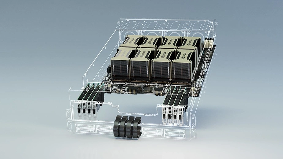
NVIDIA A100 Systems
NVIDIA packaged the A100 into purpose-built multi-GPU systems that take full advantage of the SXM form factor and NVLink interconnects.
DGX A100
The NVIDIA DGX A100 server is NVIDIA's reference AI compute platform built around eight A100 SXM GPUs. New units typically range from $150,000–$200,000, with secondary market units at $80,000 to $120,000.
The DGX Station A100 is the workstation variant for on-premises deployment where rack-mounted servers are not practical.
| Specification | Details |
|---|---|
| GPUs | 8x NVIDIA A100 Tensor Core GPUs |
| GPU Memory | 320 GB total |
| Performance | 10 petaOPS INT8 |
| NVIDIA NVSwitches | 6 |
| System Power Usage | 6.5kW max |
| CPU | Dual AMD Rome 7742 (128 cores, 2.25-3.4 GHz) |
| System Memory | 1TB |
| Networking | 8x Single-Port Mellanox ConnectX-6 VPI (200Gb/s HDR InfiniBand) 1x Dual-Port Mellanox ConnectX-6 VPI (10-200Gb/s Ethernet) |
| Storage | OS: 2x 1.92TB (M.2 NVME drives) Internal Storage: 15TB (U.2 NVME drives) |
| Software | Ubuntu Linux OS |
| System Weight | 271 lbs (123 kgs) |
| System Dimensions | Height: 10.4 in (264.0 mm) Width: 19.0 in (482.3 mm) Length: 35.3 in (897.1 mm) |
| Operating Temperature Range | 5-30°C (41-86°F) |

HGX A100
The HGX A100 is NVIDIA's OEM compute baseboard reference design, which third-party server manufacturers use to build their own A100-based systems.
HGX configurations support four or eight A100 SXM GPUs connected via NVLink, integrated into standard server chassis from Dell, HPE, and Supermicro.
| Specification | 4x NVIDIA A100 | 8x NVIDIA A100 | 16x NVIDIA A100 |
|---|---|---|---|
| HPC and AI Compute (FP16 Petaflops) | 2.5 | 5 | 10* |
| Memory | Up to 320 GB | Up to 640 GB | Up to 1,280 GB |
| NVIDIA NVLink | 3rd generation | ||
| NVIDIA NVSwitch | N/A | 2nd generation | |
| NVSwitch GPU-to-GPU Bandwidth | N/A | 600 GB/s | |
| Total Aggregate Bandwidth | 2.4 TB/s | 4.8 TB/s | 9.6 TB/s |
Running A100 Workloads on Thunder Compute
Thunder Compute offers the A100 80 GB from $1.09/hr on-demand, among the lowest rates tracked across major cloud GPU providers, with per-minute billing and no minimum commitment.
The VS Code and Cursor extensions connect directly from your IDE without SSH configuration. For a full breakdown of A100 costs across providers, see the NVIDIA A100 pricing guide.
See A100 availability and pricing on Thunder Compute →
Last Thoughts on NVIDIA A100 Specs
The A100 remains a capable GPU for fine-tuning models under 30B parameters, MIG-based multi-tenant inference, FP64 scientific computing, and cost-sensitive experimentation. For large-scale training where FP8 and the Transformer Engine matter, the H100 is typically more economical per job.
To match the right hardware to your workload, see our GPU selection guide for AI workflows.
FAQ
What memory configurations are available for the NVIDIA A100?
The A100 is available in 40 GB HBM2 and 80 GB HBM2e configurations. The 80 GB SXM variant delivers up to 2,039 GB/s of memory bandwidth.
What is an A100 GPU?
The NVIDIA A100 is a data center GPU built on Ampere architecture, released in 2020. It provides 6,912 CUDA cores and 432 third-generation Tensor Cores for AI training, inference, and scientific computing.
What is the NVIDIA DGX A100?
The DGX A100 is NVIDIA's fully integrated AI supercomputing server built around 8x A100 SXM GPUs, dual AMD EPYC CPUs, 1 TB of system memory, and 15 TB of NVMe storage.
How many GPUs are in an NVIDIA DGX A100?
The standard NVIDIA DGX A100 server has 8x NVIDIA A100 Tensor Core GPUs, all interconnected via NVLink to act as a single unified compute resource.
How much is the NVIDIA DGX A100?
New units typically range from $150,000 to $200,000. Secondary market units are generally available for $80,000 to $120,000.
What is the difference between the A100 PCIe and SXM form factors?
The PCIe variant uses a PCIe 4.0 x16 interface and draws up to 300W. The SXM4 variant mounts to NVIDIA's NVLink baseboard, supports a 400W envelope, and delivers higher memory bandwidth (2,039 GB/s vs 1,935 GB/s on the 80 GB variant).
What is Multi-Instance GPU (MIG) technology on the A100?
MIG partitions a single A100 into up to 7 isolated GPU instances, each with dedicated memory bandwidth, L2 cache, and CUDA cores. Each instance appears as a separate device to the OS, enabling multi-tenant inference on a single card.
Does the NVIDIA A100 support FP8 precision?
No. FP8 was introduced in the H100 with its fourth-generation Tensor Cores and Transformer Engine. The A100's precision ceiling for AI training is BF16 at 312 TFLOPS dense.
What is the difference between DGX A100 and HGX A100 systems?
The DGX A100 is NVIDIA's turn-key reference server with integrated CPUs and storage. The HGX A100 is the OEM baseboard that Dell, HPE, and Supermicro use to build custom A100 servers. Most cloud A100 instances run on HGX-based infrastructure.
What is structural sparsity on the A100?
Structural sparsity doubles Tensor Core throughput for models with a 2:4 sparsity pattern (exactly 2 non-zero values in every group of 4 weights). Most production transformer models do not achieve this without sparsity-aware training, so 312 TFLOPS FP16 is the practical dense baseline.
Is the NVIDIA A100 still worth using in 2026?
Yes, for fine-tuning models under 30B parameters, MIG-based multi-tenant inference, FP64 HPC workloads, and cost-sensitive experimentation. NVIDIA ceased A100 production in early 2024, but cloud availability remains strong.
What is TF32 precision on the A100?
TF32 is a 19-bit format with the numerical range of FP32 and roughly the throughput of FP16. It delivers 156 TFLOPS dense on the A100 and is the default precision for PyTorch and TensorFlow, requiring no code changes to use.
Where can I rent an NVIDIA A100 GPU?
Thunder Compute offers the A100 80 GB at $1.09/hr on-demand with per-minute billing and no minimum commitment. VS Code and Cursor extensions connect directly from your IDE.